This article was last updated on 2024-11-28, the content may be out of date.
0. Lab Document
1. Prove That the Slope of an IV Curve Corresponds with Ohm’s Law for Two Different Resistor Values
Building Block
P1-1-a
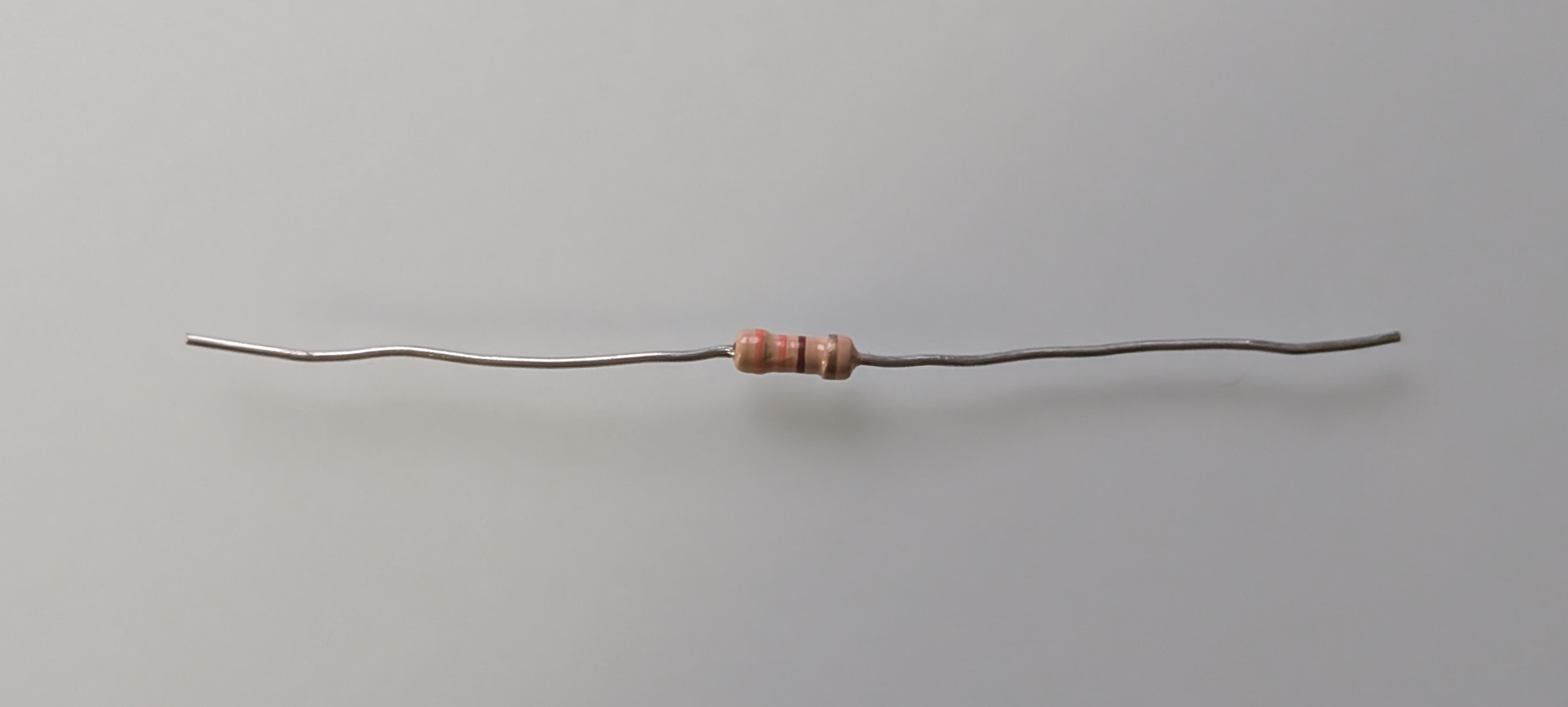
Let’s pick two resistor. The first one is
P1-1-b
4-Band Color Code: Orange, Orange, Brown, Gold
33×(1×101)=330Ω±5%
have a check
P1-1-b-2
The second one is
P1-1-c
4-Band Color Code: Brown, Brown, Red, Gold
11×(1×102)=1100Ω±5%
have a check
P1-1-c-2
Analysis
We know that IV curve means I on the y-axis and V on the x-axis of the plot. Then, it must be a linear function, because both IV don’t have powers.
Using the idea of linear function, we know the slope is ΔYΔX. Back to our case, it becomes ΔIΔV. Also, we knows the Ohm’s Law, which IV=R. So, the slope is very likely to be the resistance R.
If we take R1=10Ω, R2=100Ω (As the simulation set). We should got.
P1-2-a
If we plot them together, we got
P1-2-b
Here is the data table
I
V=IR1
V=IR2
0
0
0
0.2
2
20
0.4
4
40
0.6
6
60
0.8
8
80
1
10
100
Simulation
P1-3-a
Measurement
First we built a circuit like this
P1-4-a
this is based on the diagram from the lab document
P1-4-a-2
We only changed the R1,R2 values. Also, it’s hard to plug multimeter on the breadboard. So, we intersect the V+ circuit at the front
P1-4-b
This method is not ideal, but works.
Let’s begin
For V+=0.5V, we got
P1-4-cP1-4-c-2
To save some space and work, we just will not show each result. But here is the data
% Step 1: Enter the dataV_plus=[0,0.5,1,1.5,2,2.5,3];% V+ valuesV_R1=[0,0.142,0.238,0.358,0.463,0.572,0.632];% V(R1) valuesV_R2=[0,0.396,0.724,1.126,1.492,1.831,1.994];% V(R2) valuesI=[0,0.3,0.6,1.0,1.3,1.6,1.9]*1e-3;% I values in A (converted from mA)% Step 2: Plot the datafigure;% Plot for Resistor R1subplot(2,1,1);plot(V_R1,I,'-o');xlabel('Voltage V(R1) (V)');ylabel('Current I (A)');title('Resistor R1: Current vs Voltage');gridon;% Plot for Resistor R2subplot(2,1,2);plot(V_R2,I,'-o');xlabel('Voltage V(R2) (V)');ylabel('Current I (A)');title('Resistor R2: Current vs Voltage');gridon;
we got the plot of R1 and R2
P1-4-d
Now, let’s create a fit line for both. It’s needed to find out the slope (R=V/I). To do that, we changed the code a bit into
% Step 1: Enter the dataV_plus=[0,0.5,1,1.5,2,2.5,3];% V+ valuesV_R1=[0,0.142,0.238,0.358,0.463,0.572,0.632];% V(R1) valuesV_R2=[0,0.396,0.724,1.126,1.492,1.831,1.994];% V(R2) valuesI=[0,0.3,0.6,1.0,1.3,1.6,1.9]*1e-3;% I values in A (converted from mA)% Step 2: Fit linear regression curves% Fit for Resistor R1p_R1=polyfit(I,V_R1,1);slope_R1=p_R1(1);R_R1=slope_R1;% Resistance of R1% Fit for Resistor R2p_R2=polyfit(I,V_R2,1);slope_R2=p_R2(1);R_R2=slope_R2;% Resistance of R2% Step 3: Display the resistancesfprintf('Resistance of R1: %.3f ohms\n',R_R1);fprintf('Resistance of R2: %.3f ohms\n',R_R2);% Step 4: Plot the data and fitted curvesfigure;% Plot for Resistor R1subplot(2,1,1);plot(V_R1,I,'o');holdon;plot(polyval(p_R1,I),I,'-');xlabel('Voltage V(R1) (V)');ylabel('Current I (A)');title('Resistor R1: Current vs Voltage with Linear Fit');legend('Data','Linear Fit');gridon;% Plot for Resistor R2subplot(2,1,2);plot(V_R2,I,'o');holdon;plot(polyval(p_R2,I),I,'-');xlabel('Voltage V(R2) (V)');ylabel('Current I (A)');title('Resistor R2: Current vs Voltage with Linear Fit');legend('Data','Linear Fit');gridon;
we got a result of
1
2
Resistance of R1: 331.144 ohms
Resistance of R2: 1069.374 ohms
and the plots
P1-4-e
Check this result from multimeter’s reading of resistance
P1-4-dP1-4-d-2
Great! The actual reading is very close to the resistances we determined from your IV measurement data and the linear regression. The average % error is less than 1%
Discussion
We did a lot of discussion in each session instead of in one. This is just to make the document more logical and follows the flow. So, we will only summarize and add something not appear above.
First, we used LTSpecie to determine IV curve of two resistor R1=10Ω and R2=100Ω. (This is just for prove our Analysis, so it doesn’t match the R1=330Ω and R2=1100Ω we used later). And it matches our Analysis. Both the plot created by Excel and the values.
Then, we built a series circuit, and we know they have the same current across all components. And, the R is only related to IV. As long as we got some reading pairs, we can plot the curve. The result matches our expectation with less than 1% error. Consider our multimeter can only measure down to 0.1mV. This accuracy is amazing!
Thus, we proved That the Slope of an IV Curve Corresponds with Ohm’s Law for Two Different Resistor Values.
2. Prove the non linear IV curve for a light emitting diode
Building Block
P3-1-a
Analysis
To plot a IV curve of a diode. We need to find out a few important data.
We just plot them into a standard diode IV characteristic diagram and get
P2-2-a
Simulation
P2-3-a
The turn on voltage of 1N914 is about 0.7V
Measurement
P3-4-a
We create a trig wave like
P3-4-b
with amplitude to 5V (10 volts peak to peak), frequency to 200 Hz, and phase to 90 degrees.
Then, we use channel 1 to find out the current using the math function in scope
1
C1/330*1000
P3-4-b-2
and the IV Curve
P3-4-b-3
with this MATLAB Code,
 1
 2
 3
 4
 5
 6
 7
 8
 9
10
11
12
13
14
15
% Step 1: Import the CSV filedata=readmatrix('P2-4-c.csv');% Step 2: Extract the columnsvoltage=data(:,2);% Second column is voltage (V)current=data(:,1);% Third column is current (I)% Step 3: Plot the I-V curvefigure;plot(currentvoltage,current,'k-','LineWidth',1.5);xlabel('Voltage (V)');ylabel('Current (I)');title('I-V Curve');gridon;
we got
P2-4-c-2
Discussion
Our experimental matches the datasheet. Consider the datasheet said
VF=1.7V
IF=100mA
and we got 1.7V on 10mA this matches the datasheet curve.
3. Show / demonstrate that the differential resistance changes in different regions in the diode IV curve
Building Block
P3-1-a
Analysis
To plot a IV curve of a diode. We need to find out a few important data.
We just plot them into a standard diode IV characteristic diagram and get
P2-2-a
Simulation
P3-3-a
The turn on voltage of 1N914 is about 0.7V
Measurement
P3-4-a
We create a trig wave like
P3-4-b
with amplitude to 5V (10 volts peak to peak), frequency to 200 Hz, and phase to 90 degrees.
Then, we use channel 1 to find out the current using the math function in scope
1
C1/330*1000
P3-4-b-2
and the IV Curve
P3-4-b-3
with this MATLAB Code,
 1
 2
 3
 4
 5
 6
 7
 8
 9
10
11
12
13
14
15
% Step 1: Import the CSV filedata=readmatrix('P2-4-c.csv');% Step 2: Extract the columnsvoltage=data(:,2);% Second column is voltage (V)current=data(:,1);% Third column is current (I)% Step 3: Plot the I-V curvefigure;plot(voltage,current,'k-','LineWidth',1.5);xlabel('Voltage (V)');ylabel('Current (I)');title('I-V Curve');gridon;
we got
P2-4-c-2
Discussion
To find out at least 2 locations on the curve to show that the differential resistance changes along the I-V characteristic. We modified the code a bit to let it find out 2 random point on the plot and its slope.
% Step 1: Import the CSV filedata=readmatrix('P2-4-c.csv');% Step 2: Extract the columnsvoltage=data(:,2);% Second column is voltage (V)current=data(:,1);% Third column is current (I)% Step 3: Select two random pointsnum_points=length(current);random_indices=randperm(num_points,2);% Generate 2 unique random indices% Step 4: Extract the voltage and current values for the selected pointsV1=voltage(random_indices(1));V2=voltage(random_indices(2));I1=current(random_indices(1));I2=current(random_indices(2));% Step 5: Calculate the slopesslope1=(V2-V1)/(I2-I1);slope2=(V1-V2)/(I1-I2);% This is the same as slope1 but calculated in reverse% Step 6: Print the slopesfprintf('The slope between the randomly selected points (I1 = %.4f, V1 = %.4f) and (I2 = %.4f, V2 = %.4f) is: %.4f\n',I1,V1,I2,V2,slope1);fprintf('The slope between the randomly selected points (I2 = %.4f, V2 = %.4f) and (I1 = %.4f, V1 = %.4f) is: %.4f\n',I2,V2,I1,V1,slope2);
We got
The slope between the randomly selected points (I1 = 0.0097, V1 = 0.2959) and (I2 = 0.0036, V2 = -2.6254) is: 479.8789
The slope between the randomly selected points (I2 = 7.9784, V2 = 1.2568) and (I1 = 2.8170, V1 = 1.1975) is: 0.0115
We can see they are very different.
4. Prove That Nodal Analysis Solves Unknown Nodal Voltages in a Circuit
Building Block
P4-1-a
Analysis
P4-2-a
To make our life easier, I rewrite some equation in LATEX.
Current through a resistor:
IR=RVA−VB
Kirchhoff’s Current Law (KCL) at node B:
IR1+IR2+IR3=0
KCL at node C:
IR3+IR4=0
Expressing currents in terms of voltages. From the first equation:
R1VB−VA+R2VB+R3VB−VC=0
From the second equation:
R3VC−VB+R4VC−VD=0
Substituting known values. Given VA=5 and VD=0, the equations become:
2.5VB−VC=52VC−VB=0
Matrix form: [2.5−1−12][VBVC]=[50]
Solve them “by hand”
 1
 2
 3
 4
 5
 6
 7
 8
 9
10
% Define the matrix A and the vector bA=[2.5,-1;-1,2];b=[5;0];% Solve the system of linear equations A * x = bx=A\b;% Display the solutiondisp('The solution is:');disp(x);
we got
1
2
3
The solution is:
    2.5000
    1.2500
Thus, [VBVC]=[2.51.25]
Simulation
P4-3-a
Measurement
P4-4-a
For VC, we got
P4-4-b-1
For VB, we got
P4-4-b-2
Discussion
Node
Analysis
Simulation
Experimental
diff
%diff
VB
2.50V
2.50V
2.45V
5mV
2%
VC
1.25V
1.25V
1.22V
3mV
2.4%
Our Analysis matches the Simulation. The Experimental data has less than 2.5% error than expect, which is very less. Thus, we proved That Nodal Analysis Solves Unknown Nodal Voltages in a Circuit.
5. Prove / demonstrate your approach to designing a circuit using nodal analysis
Building Block
P5-3-a
Analysis
P5-2-a
To make our life easier, I rewrite some equation in LATEX.
Given values:
VA=3V
VC=0V
VB is unknown.
Using Kirchhoff’s Current Law (KCL) at node B:
R1VB−VA+R2VB−VC+R3VB−VC=0
Substituting the given values and resistances:
1VB−3+4VB−0+4VB−0=0
Simplifying the equation:
(VB−3)+4VB+4VB=0
Combine terms:
VB−3+2VB=0
Multiply through by 2 to clear the fraction:
2VB−6+VB=0
Combine terms:
3VB=6
Solve for VB:
VB=2
Simulation
P5-3-a
Measurement
P5-4-a-1
For VB, we got
P5-4-a
Discussion
Node
Analysis
Simulation
Experimental
diff
%diff
VB
2V
2V
1.979V
21mV
1.1%
Our Analysis matches the Simulation. The Experimental data has less than 1.2% error than expect, which is very less. Thus, we proved That Nodal Analysis Solves Unknown Nodal Voltages in a Circuit.
6. Prove the function of an op amp comparator
Building Block
P6-1-a
Analysis
A non-inverted comparator has a transfer function of
Our supply voltage are 5V and −5V, and the input is a SINE wave with amplitude of 1V, and the reference voltage is GND which is 0V
Simulation
P6-3-bP6-3-a
Measurement
P6-4-a-bP6-4-a
Discussion
Comparing our simulation to our experiment, we see that both of them are square waves with the same periods and similar amplitudes. They are fluctuating between 5 and -5, which are our supply voltages. This makes sense, because the supply voltages are the outputs of op amp comparators.
This proves our concept of an op amp comparator.
7. Prove the function of a mathematical op amp
Building Block
P8-1-a
Analysis
P8-2-a
Summing amplifier circuit has a transfer function like
Vout=−R1Rf⋅V1−R2Rf⋅V2
In our case, we want to use 50KΩ potentiometer as the resistors, so it can be adjusted according to our demand. Then, we got
VoutVout=−50K50K⋅V1−50K50K⋅V2=−V1−V2
Simulation
We just used two SINE waves with different frequencies (500Hz and 1KHz) in our simulation.
P8-3-aP5-3-b
Measurement
Then, we setup the circuit. We just connected scope channel 1 to the Vout to check it works or not
P8-4-a-b
We have Vs+=5V and Vs−=−5V
P8-4-a
We used wave generator to create to SINE waves of 500Hz and 1KHz
P8-4-b
And we checked the output wave using scope channel 1+
P8-4-c
Discussion
As we see, the shape of the output wave is exactly the same as our simulation. Both the amplitude of the output wave in the simulation and measurement is around 1.75V, and the period is the same.
Since the shape and all features of our experimental wave matches our simulation, we know this op-amp works in different voltage ranges.
This proved our concept of summer amp which is a mathematical op-amp.
8. Prove the concept of transfer functions of Two-Channel Audio Mixer
Building Block
P8-1-a
Analysis
P8-2-a
Summing amplifier circuit has a transfer function like
Vout=−R1Rf⋅V1−R2Rf⋅V2
In our case, we want to use 50KΩ potentiometer as the resistors, so it can be adjusted according to our demand. Then, we got
VoutVout=−50K50K⋅V1−50K50K⋅V2=−V1−V2
Simulation
We just used to SINE wave with different frequency (500Hz and 1KHz) to test what we expect.
P8-3-aP5-3-b
Measurement
Then, we setup the circuit. We just connect scope channel 1 to the Vout to check it works or not
P8-4-a-b
We supply Vs+=5V and Vs−=−5V
P8-4-a
And use wave generator to create to SINE wave of 500Hz and 1KHz
P8-4-b
And we checked the output wave using scope channel 1+
P8-4-c
Discussion
As we see, the shape of the output wave is exactly the same as what we simulated. Both the amplitude of the output wave in the simulation and measurement is around 1.75V, and the period is the same.